
The series so far:
- Storage 101: Welcome to the Wonderful World of Storage
- Storage 101: The Language of Storage
- Storage 101: Understanding the Hard-Disk Drive
- Storage 101: Understanding the NAND Flash Solid State Drive
- Storage 101: Data Center Storage Configurations
- Storage 101: Modern Storage Technologies
- Storage 101: Convergence and Composability
- Storage 101: Cloud Storage
- Storage 101: Data Security and Privacy
- Storage 101: The Future of Storage
- Storage 101: Monitoring storage metrics
- Storage 101: RAID
Solid-state drive (SSDs) have made significant inroads into enterprise data centers in recent years, supporting workloads once the exclusive domain of hard-disk drive (HDDs). SSDs are faster, smaller, use less energy, and include no moving parts. They’ve also been dropping in price while supporting greater densities, making them suitable for a wide range of applications.
Despite their increasing presence in the enterprise, there’s still a fair amount of confusion about how SSDs work and the features that distinguish one drive from another. Concepts such as NAND chips, multi-level cells, and floating gate technologies can be somewhat daunting if you’re still thinking in terms of rotating disks and moving actuator arms, components that have no place in the SSD.
The better you understand how SSDs operate, the more effectively you can select, deploy, and manage them in you organization. To help with that process, this article introduces you to several important SSD concepts so you have a clearer picture of the components that go into an SSD and how they work together to provide reliable nonvolatile storage.
Bear in mind, however, that an SSD is a complex piece of technology and can easily justify much more in-depth coverage than what a single article can offer. You should think of this as an introduction not a complete treatise, a starting point for building a foundation in understanding the inner workings of your SSDs.
Introducing the NAND Flash SSD
Like an HDD, an SSD is a nonvolatile storage device that store data whether or not it is connected to power. An HDD, however, uses magnetic media to store its data, whereas the SSD uses integrated electronic circuitry to retain specific charge states, which in turn map to the data bit patterns.
SSDs are based on flash memory technologies that enable data to be written, read, and erased multiple times. Flash memory comes in two varieties: NOR and NAND. Although each offers advantages and disadvantages (a discussion beyond the scope of this article), NAND has emerged as the favored technology because it delivers faster erase and write times. Most contemporary SSDs are based on NAND flash, which is why it’s the focus of this article.
An enterprise SSD contains multiple NAND flash chips for storing data. Each chip contains one or more dies, and each die contains one or more planes. A plane is divided into blocks, and a block is divided into pages.
Of these, the blocks and pages are the greatest concern, not because you configure or manipulate them directly, but because of how data is written, read, and erased on a NAND chip. Data is read and written at the page level, but erased at the block level, as illustrated in Figure 1.
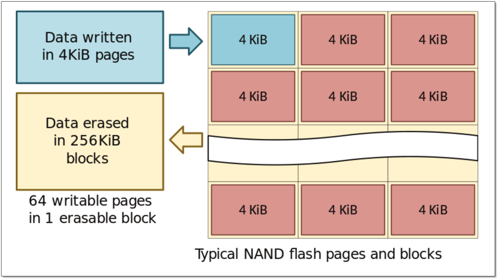
Figure 1. Writing and erasing data in a NAND flash SSD (image by Dmitry Nosachev, licensed under Creative Commons Attribution-Share Alike 4.0 International)
In this case, each page is 4 kibibytes (KiB) and each block is 256 KiB, which equals 64 pages per block. (A kibibyte is 1024 bytes. Kibibytes are sometimes used instead of kilobytes because they’re more precise. A kilobyte can equal 1000 bytes or 1024 bytes, depending on its usage.) Each time the SSD reads or writes data, it does so in 4-KiB chunks, but each time the drive erases data, it carries out a 256-KiB operation. This write/erase difference has serious consequences when updating data, as you’ll see later in the article.
Inside the NAND Cell
A page is made up of multiple cells that each hold one or more data bits. A data bit is represented by an electrical charge state, which is determined by the electrons trapped between insulator layers within the cell. Each bit is registered as either charged (0) or not charged (1), providing the binary formula needed to represent the data.
Today’s NAND flash chips use either floating gate cells or charge trap cells. Until recently most NAND flash relied on floating gate technologies, in which the electrons are trapped between two oxide layers in a region called the floating gate. The bottom oxide layer is thin enough for electrons to pass through when voltage is applied to the underlying substrate. Electrons move into the floating gate during a write operation and out of the floating gate during an erase operation.
The challenge with the floating gate approach is that each time voltage is applied and electrons pass through the oxide layer, the layer degrades slightly. The more write and erase operations, the greater the degradation, until eventually the cell might no longer be viable.
Bear in mind, however, that SSD technologies have come a long way, making them more reliable durable, while being able to deliver greater performance and store more data. At the same time, they keep coming down in price, making them much more competitive in price.
Vendors continue to explore new technologies to continue to improve SSDs. For example, several vendors are now turning to charge trap technologies in their NAND cells. Charge trap cells are similar to floating gate cells except that they use different insulator materials and methodologies to trap the electrons, resulting in cells that are less susceptible to wear. That said, charge trap technologies come with their own reliability issues, so neither approach is ideal.
There is, of course, much more to floating gate and charge gate technologies, but this should give you some idea of what’s going on, in the event you come across these terms. But know too that gate technologies are only part of the equation when it comes to understanding the NAND cell structure.
In fact, the bigger concern when evaluating SSDs is the number of bits stored in each cell. Today’s SSDs accept between one and four bits per cell, with a correlated number of charge states per cell, as shown in the following table. Note that vendors are also working on five-bit cell flash—dubbed penta-level cell (PLC)—but the jury is still out on this technology.
|
Cell type |
# of data bits |
# of charge states |
Possible binary values per cell |
|
Single-level cell (SLC) |
1 |
2 |
0, 1 |
|
Multi-level cell (MLC) |
2 |
4 |
00, 01, 10, 11 |
|
Triple-level cell (TLC) |
3 |
8 |
000, 001, 010, 011, 100, 101, 110, 111 |
|
Quad-level cell (QLC) |
4 |
16 |
0000, 0001, 0010, 0011, 0100, 0101, 0110, 0111, 1000, 1001, 1010, 1011, 1100, 1101, 1110, 1111 |
As the table shows, the more bits per cell, the greater the number of available charge states per cell, and the more charge states, the greater the number of available binary values, which translates to greater density. Not only does this mean packing in more data on each chip, but it also means more affordable drives.
Unfortunately, when you start squeezing more bits into each cell, performance suffers and the cells wear out faster. A QLC drive might hold more data and be a lot cheaper, but an SLC drive will deliver the best performance and last the longest, although at a greater price.
In addition to squeezing in more bits per cell, vendors have also been shrinking cells to fit more of them on each chip. Although this increases data density, this can lead to electrical charges leaking from one cell to another, so additional techniques must be leveraged to avoid data corruption and preserve data integrity. But vendors have an answer for this as well: 3-D NAND.
In the 3-D approach, vendors back off from shrinking cells and instead stack cells on top of each other in layers, creating chips that can hold significantly more data. When combined with multi-bit technologies such as MLC or TLC, 3D NAND makes it possible to increase chip densities beyond anything before possible, without sacrificing data integrity. For example, Samsung’s sixth-generation V-NAND chip combines 3-D and TLC technologies to store up to 256 Gb of data across 136 layers of cells. (For more information about performance-related concepts, refer to the second article in this series.)
The SSD Components
NAND chips are at the heart of the SSD, carrying out the drive’s main function of storing data. But an SSD also includes several other important components which work together to facilitate the read, write, and erase operations.
Figure 2 shows an HGST Ultrastar SSD that holds 1.6 TB of data. Although the NAND chips are covered by a label, you can see that the circuit board is filled with a variety of other components.
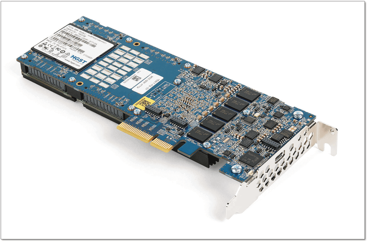
Figure 2. HGST Ultrastar SN150 Series NVMe/PCIe solid-state drive (photo by Dmitry Nosachev, licensed under Creative Commons Attribution-Share Alike 4.0 International)
To the right of the connector pins, the device hosts five Micron DRAM chips, neatly arrayed from bottom to top. The chips serve as a cache for improving write operations and maintaining system data. Unlike the NAND chips, the cache is volatile (non-persistent) and used only as a temporary buffer. In other words, although the buffered data won’t survive a loss of power, the drive will deliver better performance when it’s running.
The HGST drive has a 2.5-inch form factor and provides a Peripheral Component Internet Express (PCIe) interface. It also supports the Non-Volatile Memory Express (NVMe) protocol for maximizing the benefits of the PCIe interface. (For more information about form factors, interfaces, and protocols, refer to the first article in this series.)
You can see the PCIe interface connector in Figure 1, jutting out from the side of the circuit board. You can also see it in Figure 2, which shows the front side of the HGST drive, covered mostly by the heat sink.
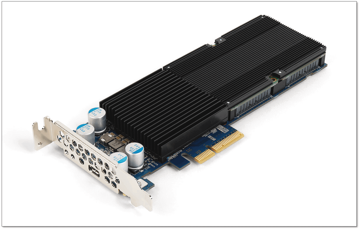
Figure 3. HGST Ultrastar SN150 Series NVMe/PCIe solid-state drive (photo by Dmitry Nosachev, licensed under Creative Commons Attribution-Share Alike 4.0 International)
SSD configurations can vary considerably from one to the next, so don’t assume that others will look like the HGST drive. I picked this one because it provides a good example of a NAND flash SSD.
Despite the differences between SSDs, they all include NAND chips, conform to specific form factors and interface standards, and typically provide some type of cache to serve as a memory buffer. (All enterprise storage devices—HDD and SSD—provide built-in volatile cache.) An SSD also includes a controller for managing drive operations and firmware for providing the controller with the instruction sets necessary to carry out those operations.
Reading and Writing Data
As noted earlier, reading and writing data occur at the page level. Reading data is a fairly straightforward operation. When the drive receives a request for data, the controller locates the correct cells, determines the charge states, and ensures that the data is properly returned, using buffer memory as necessary. The entire process has little long-term impact on the drive itself.
Writing data is a programming operation that sets the data bits to the desired charge state, a process orchestrated by the controller. – Writing data to a page for the first time is nearly as straightforward as reading data. The process grows more complex when modifying that data, which requires that it first be erased and then rewritten, a process commonly referred to as a program/erase cycle (P/E cycle).
During a typical P/E cycle, the entire block containing the targeted pages is written to memory. The block is then marked for deletion and the updated data rewritten to another block. The actual erase operation occurs asynchronously in order to optimize performance.
The controller coordinates the erase and write processes, using advanced data management algorithms. Even if only a single change on a single page needs to be recorded, an entire P/E cycle is launched. The block is marked for deletion and all its data rewritten.
The controller erases the block when it’s needed or as part of an optimization process. When erasing the block, the controller sets every bit in every cell to 1. After that, data can be written to any page in the block. However, if any bits in a page are set to 0—even if only one—the entire page is off-limits to writing data.
As an SSD starts filling up, the writing and rewriting operations become more complex and start to slow down. The controller must find places to store the data, which can involve erasing blocks marked for deletion, moving and consolidating data, or performing multiple P/E cycles. The fuller the drive, the more extensive these operations, which is why performance can start to degrade as a drive reaches capacity.
Because of the many P/E cycles, more data is routinely written to the drive than the amount being modified, a characteristic commonly called write amplification. For example, updating a simple 25-KB text file might result in 250 KB of data being written, causing additional wear on the cells.
A flash SSD can support only a limited number of P/E cycles before it fails. The more bits squeezed into each cell, the fewer that number and the faster the time to failure. For example, an MLC drive might support up to 6,000 P/E cycles per block, but a TLC drive might max out at 3,000.
As P/E cycles start adding up, cells start failing. For this reason, SSDs employ several strategies to extend a drive’s lifespan, assure reliability, and maintain data integrity, including:
- Wear leveling: A controller-based operation for distributing P/E cycles evenly across the NAND chips to prevent any cells from premature failure.
- TRIM command: An operating system command for consolidating a drive’s free space and erasing blocks marked for deletion, which can improve performance and minimize write application.
- Over-provisioning: Extra drive space reserved for management processes such as wear leveling and for reducing the extra write amplification that occurs when a drive gets too full.
- Caching: A process of storing data in memory to boost performance and, when used effectively, minimize P/E cycles.
- Error-correction code (ECC): A process for checking data for errors and then, if necessary, correcting those errors.
An SSD might also incorporate strategies for improving performance. For example, flash drives implement garbage collection, a background process for moving, consolidating, and erasing data. There’s some debate about whether garbage collection adds write amplification or reduces it. It depends on how the garbage collection operations are implemented and the quality of the algorithms used to carry out these operations.
SSD firmware updates might also address performance, reliability, and integrity issues, along with other types of issues. Whenever you install a new SSD, one of the first steps you should take is to ensure that you’re running the latest firmware. These are not necessarily the only tactics that a drive will employ, but they represent some of the most common.
Much More to the SSD
The information covered here should give you a sense of how NAND flash SSDs work. At the same time, you no doubt also realize that SSDs are extremely complex devices and that what I’ve touched upon barely scratches the surface. Even so, you should now have a more solid foundation for moving forward.
Keep in mind, however, that memory technologies are quickly evolving, with some redefining how we think of memory and storage. For example, an Intel Optane drive can store data like NAND but operate nearly as fast as DRAM, bridging the gap between traditional storage and traditional memory. Whether Optane or a similar technology will replace flash is yet to be seen, but no doubt something will, at which point we’ll be having a very different discussion.


Load comments